Key points
- Resonac makes a 300mm silicon carbide wafer
- Why bigger wafers matter for chip costs
- How far it is from production
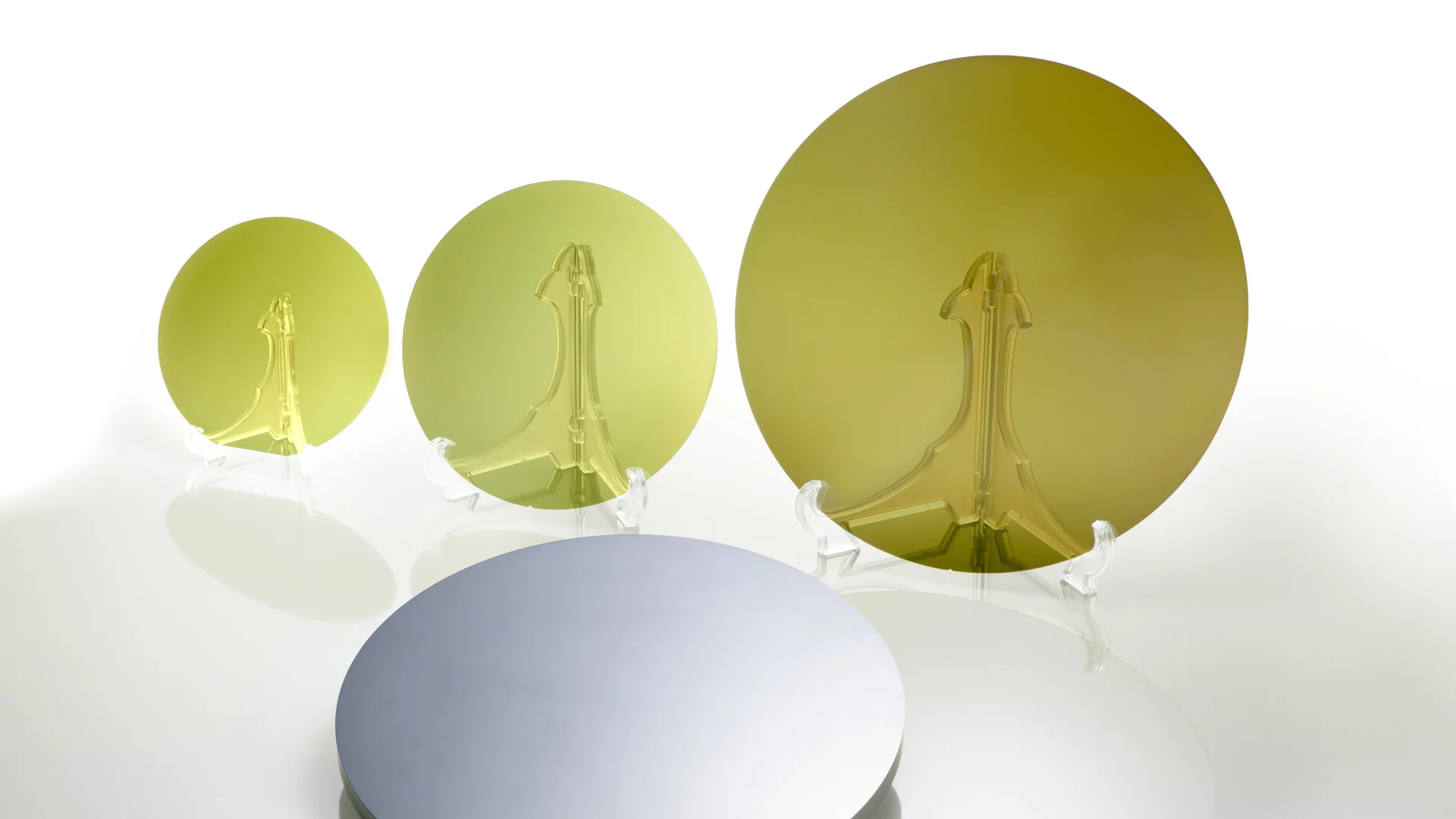
Resonac Holdings (4004.T) has grown and processed a 300mm silicon carbide wafer, expanding the size of the wafers used to make power chips for electric vehicles and data centers. Resonac is the first company in Japan to make one.
A 300mm (12-inch) wafer has four times the surface area of a 150mm (6-inch) wafer, creating room for more chips per wafer. That could lower manufacturing costs per chip, though the savings depend on production costs and how many usable chips each wafer yields. Resonac announced the wafer on September 15.
It is not the first 300mm silicon carbide wafer. China's SICC unveiled a 300mm substrate in November 2024, and Wolfspeed (WOLF) produced a 300mm wafer in January. Resonac describes its wafer as "one of the world's largest SiC substrate sizes currently under development."
Why silicon carbide matters
Silicon carbide power chips waste less energy and run cooler than chips made from ordinary silicon, according to Resonac. They are used in electric vehicles and renewable energy systems, and increasingly in power supplies for data centers.
Resonac mainly supplies 150mm silicon carbide wafers today and has begun shipping 200mm ones. The company also says single-crystal silicon carbide could be used in heat-spreading and advanced packaging substrates for chips in AI servers.
How far it is from production
The 300mm wafers remain under development. Resonac did not give a timeline for commercial production. The work draws on a research project under Japan's Green Innovation Fund, run by the government-backed New Energy and Industrial Technology Development Organization.
In another silicon carbide development, Navitas Semiconductor (NVTS) said Monday that the U.S. Army selected the company to develop a manufacturing process for 10 kV silicon carbide chips.
Cover photo: Resonac.